Quantitative Prediction of Power Loss for Damaged Photovoltaic Modules Using Electroluminescence


Institute for Photovoltaics and Research Center SCoPE, University of Stuttgart, 70569 Stuttgart, Germany
*
Author to whom correspondence should be addressed.
Energies 2018, 11(5), 1172; https://doi.org/10.3390/en11051172
Submission received: 13 April 2018
/
Revised: 2 May 2018
/
Accepted: 4 May 2018
/
Published: 7 May 2018
(This article belongs to the Special Issue PV System Design and Performance)
Abstract
:Electroluminescence (EL) is a powerful tool for the qualitative mapping of the electronic properties of solar modules, where electronic and electrical defects are easily detected. However, a direct quantitative prediction of electrical module performance purely based on electroluminescence images has yet to be accomplished. Our novel approach, called “EL power prediction of modules” (ELMO) as presented here, used just two electroluminescence images to predict the electrical loss of mechanically damaged modules when compared to their original (data sheet) power. First, using this method, two EL images taken at different excitation currents were converted into locally resolved (relative) series resistance images. From the known, total applied voltage to the module, we were then able to calculate absolute series resistance values and the real distribution of voltages and currents. Then, we reconstructed the complete current/voltage curve of the damaged module. We experimentally validated and confirmed the simulation model via the characterization of a commercially available photovoltaic module containing 60 multicrystalline silicon cells, which were mechanically damaged by hail. Deviation between the directly measured and predicted current/voltage curve was less than 4.3% at the maximum power point. For multiple modules of the same type, the level of error dropped below 1% by calibrating the simulation. We approximated the ideality factor from a module with a known current/voltage curve and then expand the application to modules of the same type. In addition to yielding series resistance mapping, our new ELMO method was also capable of yielding parallel resistance mapping. We analyzed the electrical properties of a commercially available module, containing 72 monocrystalline high-efficiency back contact solar cells, which suffered from potential induced degradation. For this module, we predicted electrical performance with an accuracy of better than 1% at the maximum power point.
1. Introduction
Electroluminescence (EL) imaging is a powerful tool to delineate the local and overall electrical and electronic properties of photovoltaic (PV) modules [1,2,3,4,5,6]. Mapping of EL allows for the characterization of not only single solar cells, but also modules and even complete module strings in large area photovoltaic systems. Thus, this method is capable of detecting electronic or electrical effects on the length scale, from micrometers to tens of meters, depending on the spatial resolution of the camera (and on the diffusion length of carriers). Most commonly, EL images provide qualitative information about the pure existence of defective parts of cells or modules in a photovoltaic system [1,2]. Sometimes, from the shape of luminescence patterns it is also possible to conclude on the type of defects [6]. Moreover, if EL measurements are combined with other characterization techniques, it is sometimes also possible to quantitatively predict the electrical performance of the cell, module, or module string [5]. However, so far it has not been possible to make quantitative predictions on the performance of cells, modules, or module strings, just from EL measurements alone.
This contribution presents a novel method for the quantitative prediction of the electrical properties (i.e., the current/voltage curve) of all cells in a photovoltaic module, just from EL measurements. The method is particularly appropriate for PV modules, which can be damaged by mechanical impact, such as hail, wind, snow, and earthquakes, and/or for modules which suffer from potential induced degradation (PID). In both cases, either the series resistances of the cell fragments or the shunt resistance of a total cell have changed when compared to the original, undamaged state. For these cases, we are able to convert electroluminescence images into either a series resistance or a parallel resistance map. With these maps, together with data from the original data sheet of the undamaged module, we are then able to predict the complete current/voltage curve of the damaged modules. Therefore, we are also able to quantitatively predict the electrical power loss of the damaged modules. The current/voltage curves, which we predict by means of our novel ELMO method are in excellent agreement with the directly measured curves.
2. Modelling Principle
2.1. Basic Principle of the ELMO Method
The electroluminescent signal in solar cells or modules stems from the recombination of electrons and holes, which, due to applied voltage at the junction, are in non-equilibrium. The luminescence signal therefore locally originates from the diode itself as well as from the bulk of the material within a radial distance of the order of a diffusion length. Luminescent intensity depends on the current across the junction. The junction current, in turn, depends on:
- The junction voltage (which is only part of the externally applied voltage due to series resistances);
- The ideality factor and saturation current density of the diode; and
- The shunt currents that circumvent the diode.
Our ELMO method makes use of two independent principle ideas for modelling mechanically damaged modules as well as PID affected modules.
2.1.1. Series Resistance Mapping of Mechanically Damaged Modules
The mechanical damage of modules, in a first order approximation, does not change the quality of the junction (ideality factor, saturation current density, shunt resistance), but only the series resistances due to broken contact fingers and bus bars, for example. Therefore, it is possible to generate a series resistance map just by comparing two EL images. The first image is taken at a relatively low current (with all the external voltage dropping across the junction). As introduced by Potthoff et al. [3], in this case, the highest luminescence intensity in each cell measures the voltage share (operating voltage) of each cell to the total applied voltage. Potthoff et al. used this method to calculate the overall module series resistance from a second EL image with higher current injection (with parts of the voltage also dropping at the local series resistances as well as connecting resistances between the cells). Here, we extended the approach of Potthoff et al.
We determined the maximal possible luminescence of each cell at high current injection, as predicted from the low current EL image without series resistance dependence.
Consequently, each local series resistance was directly related to the reduced luminescence compared to the maximal luminescence in each cell. In addition, in the high current EL image, the series resistance at the location of maximal luminescence was no longer negligible.
Therefore, we determined the resistance at the location of maximal luminescence and thereby quantified all local series resistance of the cell in respect to the local resistance at the location of maximal luminescence.
For this purpose, based on data sheet information, we calculated the mean series resistance of the originally defect-free cell. We assumed that in each cell at least one partial area persisted with a good connection to the bus bars, which was appropriately described by the respective portion of the mean series resistance of the defect free cell. Therefore, the highest EL signal of each cell in the high current EL image represented the lowest series resistance in this particular cell. These lowest series resistances were in a constant ratio to the mean resistance of the defect-free cell. Therefore, in each cell we quantified its local series resistances relative to the lowest series resistance (i.e., the mean resistance of the defect-free cell) by evaluating its local luminescence intensities relative to the maximal luminescence of the particular cell.
2.1.2. Parallel Resistance Mapping of PID Modules
The PID of modules, within the most simplified approximation, does neither change the junction (ideality factor, saturation current density) nor the series resistances, but the parallel resistances of the constituting cells. As a consequence, if there is still one defect free cell left in the module, we are able to calculate all parallel resistances with respect to this defect free cell, which exhibits the highest mean luminescence signal in the low current EL image. This reference cell calibrates the EL intensities of all other cells, at a relatively low current with all the external voltage dropping across the junction. Therefore, the reduction in luminescence of the PID affected cells originates from leakage/shunt currents through the parallel resistances. As a consequence, the low current EL image directly allows for the quantification of the parallel resistance of each cell and maps the parallel resistances of a PID module.
2.2. Mathematical Description of ELMO
2.2.1. Series Resistance Mapping from EL Images
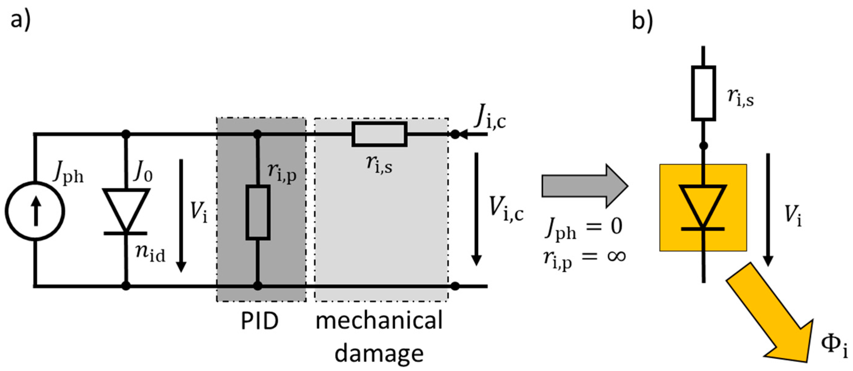
The simplest and most common approach for describing the electrical properties of solar cells and even total PV modules is the evaluation of the one-diode model. Figure 1a shows the equivalent circuit of the one-diode model, with the photo current source providing the photo generated current density , series resistance , the diode parameters with the ideality factor and saturation current density as well as the parallel resistance , which reproduces the current(I)/voltage(V) curve of each solar cell with cell index i in a module with a total number N of solar cells. Further simplified for a module in the dark ( 0), Figure 1b shows the simplified equivalent circuit in the case of an idealized parallel resistance . The junction voltage generates the luminescence intensity
Specific defects such as mechanically damaged and cracked solar cells only change the local series resistance , i.e., the equivalent connecting resistance of partially separated segments. The diode parameters ( and ) are assumed to be unchanged and still the same as for the originally defect free solar cells. In contrast, defects like PID, in the simplest approximation, only change the parallel resistance of a cell.
These assumptions allow us to calculate the change in series resistance or parallel resistance directly from EL images, which essentially map the local junction voltages . Each luminescence intensity captured in each pixel of an EL image or even larger segments of approximately the same intensity are described with equivalent circuits, as shown in Figure 1a,b.
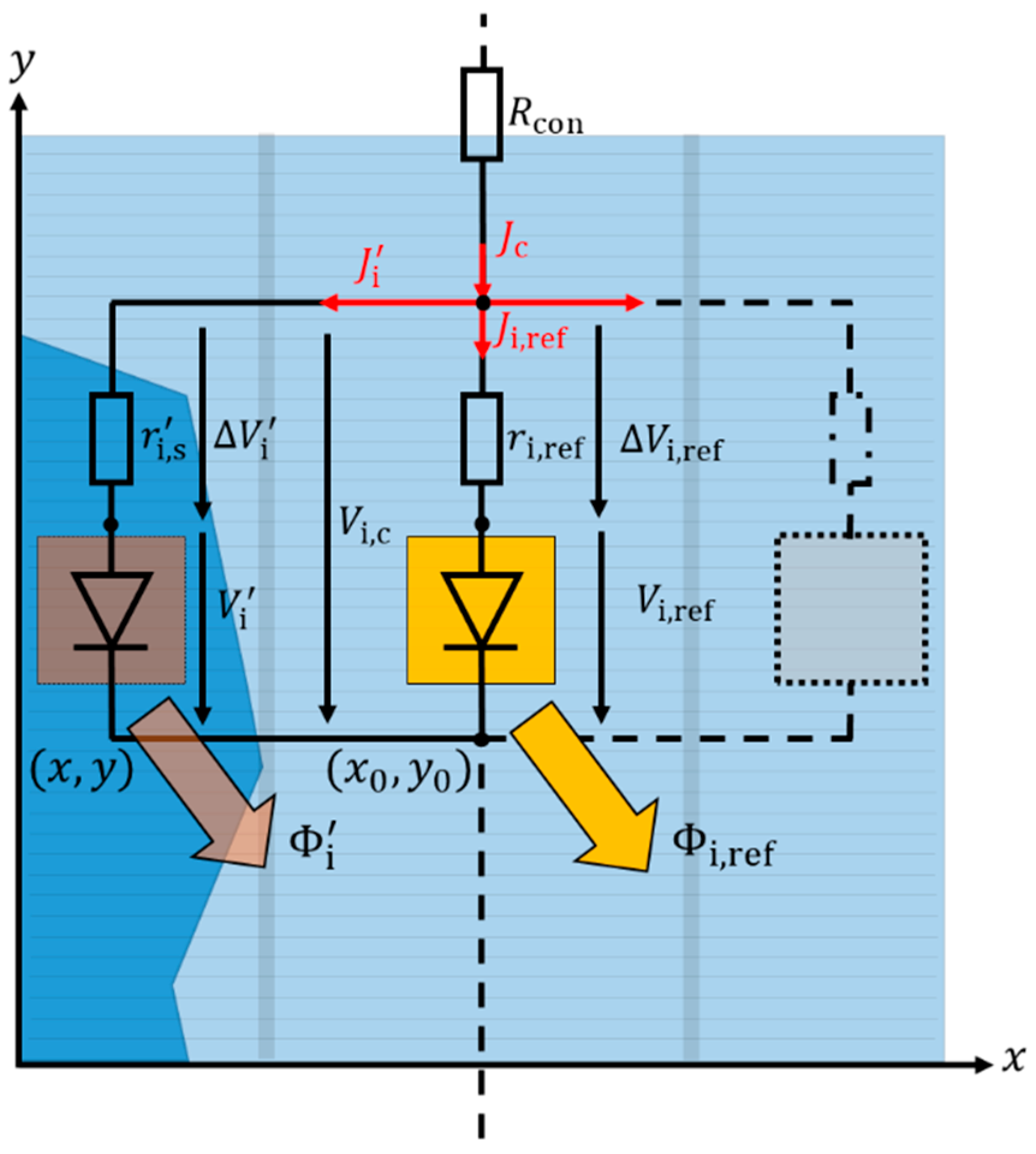
Figure 2 shows the parallel connected spatial distribution of equivalent circuits for evaluating the local luminescence intensities inside a solar cell i with cell voltage . The cell current density is identical for all series connected cells inside the module.
Since the local luminescence intensities,
captured in an EL image depend exponentially on the local junction voltage of cell i, an increase in local series resistance decreases the local junction voltage and therefore also decreases the local luminescence intensity .
The index i represents the cell number inside the module up to the total number N of cells. Each locally assigned value is indicated by an upper quote throughout this paper. Depending on the spatial resolution of one cell in the EL image, each local value is also mapped by x and y inside each cell i.
Potthoff et al. proposed that in each cell, even with cracks and inactive areas, there is always one spot with good connection to the bus bars [3]. As a consequence, the series resistance at this location is the lowest series resistance. Therefore, this part of the cell shows the highest luminescence intensity in the EL image. If this EL image is generated with low current density (approximately of short circuit density [3]), the voltage drops are negligible across the local reference series resistance as well as connecting resistances between the cells.
Based on this simplification, Potthoff et al. calculated from the low current EL image the contribution of each cell to the overall module voltage used for generating the EL signal. Their evaluation of the low current EL image quantitatively connected the local luminescence (), measured in arbitrary units, to the local junction voltages of each cell i in the module with the calibration factor:
calculated with the reference luminescence intensity () of each cell i up to the total number N of cells, the module voltage for generating the EL signal and the thermal voltage [3].
At this point, we extend Potthoff et al.’s approach. For EL images from higher current injections (30% ), the local series resistance, even at the brightest spot, is no longer negligible. Though, if the series resistance at the brightest spot is well known, all other series resistances can be calculated in relation to the reference series resistance at the brightest spot. Here, we assume that this reference resistance remains unchanged by the structural defect and is therefore directly proportional to the mean series resistance of the cell in the originally produced defect free module (data sheet module).
Our approach calculates the mean series resistance of undamaged and all identical cells from the data sheet of the undamaged PV module. The mean series resistance is derived from a lumped one-diode model with the total module resistance , the cell area and the number of cells N that represents the data sheet information of the module.
The reference series resistance at the brightest spot always represents the minimal series resistance of the cell. This minimal resistance , is calculated taking the statistical deviation from of the mean resistance of the defect free cell into account. For the similar spatial fluctuation of the series resistance of defect free cells, the statistical deviation is assumed to be constant and identical for all cells.
Based on the equivalent circuit of Figure 2, we evaluate the local luminescence intensities () in each cell i. The influence of parallel resistance is neglected. Therefore, the total local current density () is equal to the total current through the local diode and thereby proportional to the local luminescence ().
Using the exponential dependence between the local current density () and the local voltage (), the local luminescence intensities () as well as the reference luminescence () are proportional to their local current densities,
at each local region () of a cell i and the reference region () of the same cell. Therefore, the voltage difference,
is defined with respect to the local luminescence intensities (). Combining Equations (3) and (4) results in:
for each region of interest () with the local series resistance () in relation to the reference region () with the local series resistance (). As a result, the local series resistance,
for each individual cell i is calculated combining Equations (3) and (5). The thermal voltage , the ideality factor , as well as the saturation current density are assumed to be identical and constant for all cells and unrelated to the structural defect. Thereby, all local luminescence intensities () from the high current EL image (compare Figure 1a) are transposed into the series resistance mapping () further discussed in Section 2.3.
Since the statistical deviation of series resistances is at first unknown and itself depends on the calculated series resistance map , we use the bisection method to calculate the factor from Equation (6) iteratively.
We start from a guessed initial statistical deviation and calculate the module series resistance map from the high current EL image. Then, we derive the mean series resistance of one defect free cell from the sum of all local series resistances divided by the number of pixels per cell. Using the bisection method, we adjust the statistical deviation iteratively until the mean series resistance derived from series resistance map equals the series resistance of one defect-free cell derived from the data sheet. This calibration of the series map with respect to the data sheet allows for the transposition of the EL image into a series resistance input for the simulation model, shown in Section 2.3.
However, the resistance map as well as the mean series resistance derived from the data sheet, depend on the assumed ideality factor . Therefore, all further simulated results need to be evaluated in relation to an ideality factor expectation interval. As a further approximation, the ideality factors of all cells are assumed to be identical. Nevertheless, these approximations already lead to excellent results when comparing simulated and measured I/V curves.
2.2.2. Parallel Resistance Mapping from EL Images
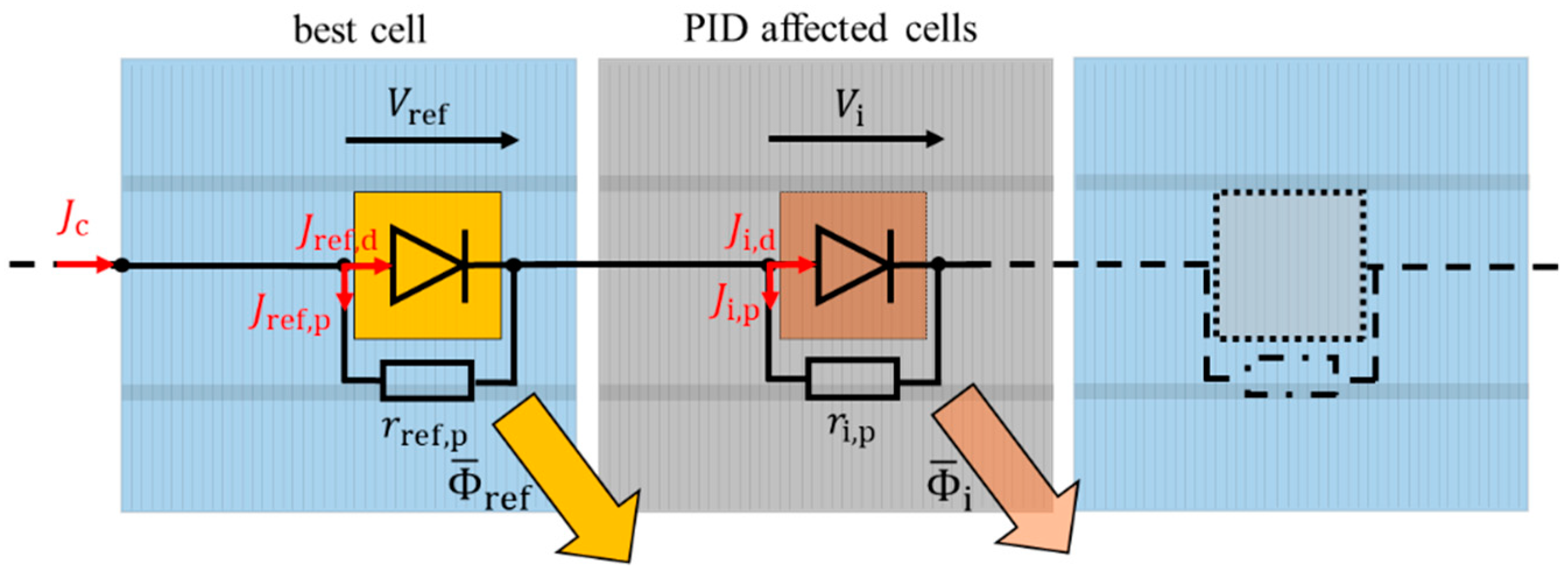
Figure 3 shows the equivalent circuit for evaluating the mean luminescence of each cell i in relation to the maximal mean luminescence of all cells. Here, the same principle approach as shown in Section 2.2.1 evaluates the total parallel resistance of each cell i. However, this parallel resistance approximation (PRA) only holds true if the evaluated defect type is limited to change in parallel resistance and is not additionally influencing the local series resistance of the cell.
The connecting resistance between the cells and the local series resistance is neglected for the cell current density , used for generating the low current EL image. The cell current being the same for every in series connected cell, is divided into parallel resistance current density and local diode current density . The diode current density of a cell i is proportional to mean luminescence , defined analogously by Equation (3). Solving for the parallel resistance current density,
at the reference cell with the maximal mean luminescence and using Equations (1) and (3) results in the relation,
In this case, taking into account the reference parallel resistance , the calibration factor,
is calculated by solving Equation (8) with the main branch of the Lambert-W function. Using Equation (8) analogously for the mean luminescence of all other cells instead of the reference cell, the parallel resistance,
is calculated for each cell i. The cell current is well-known, since it needs to be adjusted and measured to generate the low current EL image. The recombination current density is calculated from the data sheet information of the PV module and only the ideality remains a scalable parameter. Again, all further simulated results will be evaluated in relation to an ideality factor expectation interval.
2.3. Series Resistance Segmentation and Module Simulation
Figure 4a shows the high current EL image and Figure 4b the low current EL image of a photovoltaic module with 60 multicrystalline silicon solar cells (cell area = 243 cm2). In both images, darker regions with lower EL intensity indicate cracked cells with fully or partially disconnected cell areas.
To quantify the impact of those structural defects we convert the luminescence image shown in Figure 4a into a series resistance map. Based on series resistance mapping, our simulation model predicts the overall power loss induced by the change in local series resistance of the individual cells with all cells connected in series.
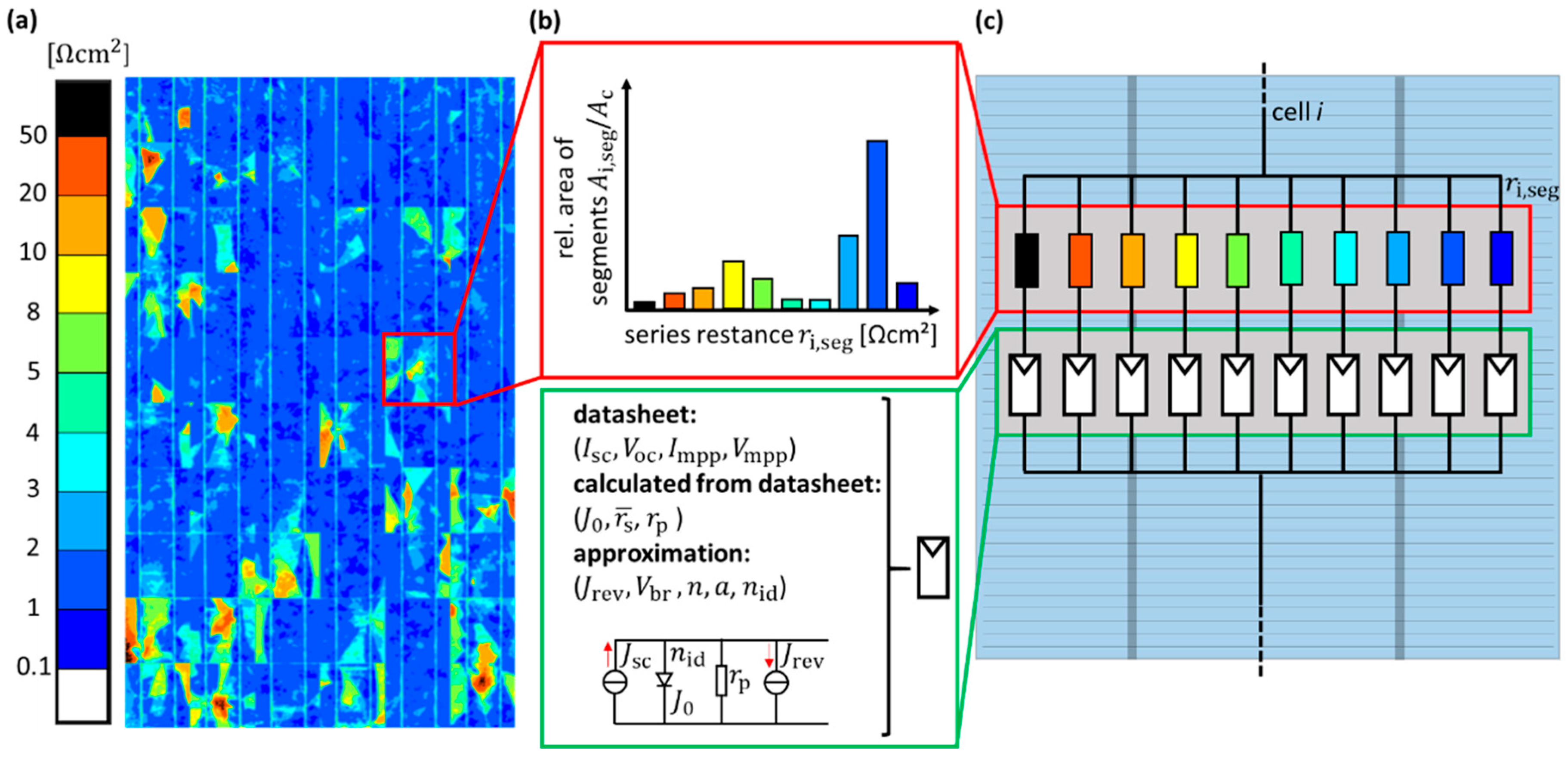
Starting from the series resistance map, Figure 5 shows the simulation principle for calculating the predicted power loss compared to the data sheet performance. Figure 5a shows the series resistance map with colored segmentation categories in units of Ω cm2. The space in between the cells is cut out and excluded for the series resistance segmentation. Figure 5b (red box) qualitatively shows the histogram of categorized series resistances () of one cell i with the relative area of a segment, as a share of the total cell area .
The mean series resistance in each segment is used for the simulation model shown in Figure 5c, predefined into ten segments. Each series resistance is weighted by its relative area . All constant diode model parameters (green box in Figure 5b) are directly derived from the data sheet or calculated from a one-diode model. Figure 5c shows the resulting simulation model for cell i.
All cells i = 1, 2, …, N, with a total number N of cells, are connected in series and simulated with the bypass diode configuration of the module (typically 20 or 24 cells anti-parallel connected to a bypass-diode).
Note, fully and partially disconnected cell areas potentially limit the short circuit current density of the cell. In this case, highly damaged cells with a large part of the cell being disconnected, are no longer acting as a current source. These cells operate under reverse bias () and limit the power output of the module, depending on their interaction with the bypass diodes.
Therefore, the reverse characteristics for describing the reverse current density under reverse bias () are numerically modelled as originally introduced by Bishop [8] and further applied by Quaschning [7]. As proposed by Quaschning, for describing multicrystalline solar cells we incorporate the breakdown voltage = −15 V, as well as the avalanche effect under reverse bias by the non-linear multiplication factors = 2.3 × 10⁻³ and 1.9. Again, we assume identical cells with the same breakdown model unrelated to the defects.
Finally, by evaluating the ideality factor expectation interval (identical ideality factors for all cells), in this case for the ideality factor of multicrystalline silicon solar cells, we find excellent agreement compared to measured results.
To evaluate PID modules, the simulation model is further simplified. Since the change in parallel resistance influences each total cell i, no segmentation is needed. Therefore, the series resistance of each cell i is extracted in a straightforward manner from the data sheet and only the overall parallel resistance of each cell is varied in the simulation model based on Equation (10).
3. Experimental Results
3.1. Hail-Damage Modules with Cracked Cells
As a reference measurement, a multicrystalline silicon PV module (module A) was characterized via the measured I/V curves of each individual cell of this module. The characterized module with 60 multicrsystalline cells (data sheet maximum power = 230 Wp) was already installed prior to the experiments and showed multiple cracked cells after on-site hail impacts (compare Figure 4a). The bus bars in between the cells were reached by drilling small holes through the backsheet encapsulation. At the interconnections between the cells, the positive and negative contact of each cell, was accessible. A Keithley 2651a source-meter captured the I/V curves of each cell, as well as of the total module, while a halogen-lamp solar simulator irradiated the module with the equivalent solar irradiance = 600 W/m2 (0.6 suns). All I/V curves were transposed into standard test condition (STC) equivalent electrical characteristics. The EL images were captured by a cooled Si-CCD camera (FLI MicroLine ML8300M, 8.3 Megapixel) and downsampled to a fixed resolution of 100 × 100 pixel/cell.
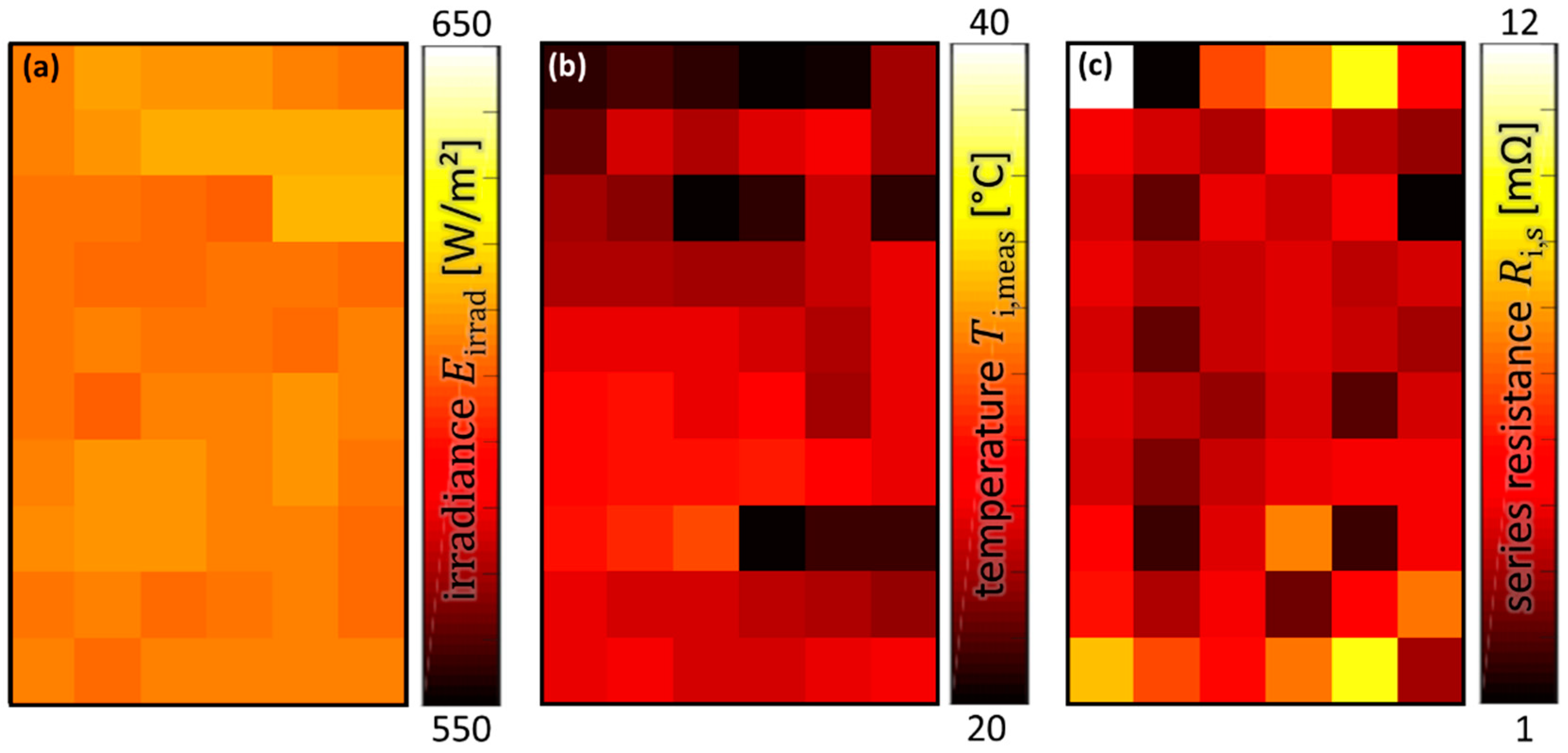
Figure 6a shows the measured irradiance on the total module and Figure 6b the measured temperature during the acquisition of the I/V curves for each cell i. Figure 6c shows the calculated series resistance , numerically derived from a two-diode equivalent circuit which reproduced the I/V curves for each cell i. These parameters are mandatory and used for deriving the STC characteristics of all cells.
Based on the temperature coefficient of the total module, the open circuit cell voltages were transposed into temperature values . The temperature was calibrated by a reference measurement at room temperature immediately before performing all further measurements. Here, we assumed that the cells maintained room temperature during measurement, without any temperature drift. Therefore, depending on the location of the cell inside the module, two tracked open circuit voltages were used to determine each cell temperature during I/V measurements. Irradiance was measured via a reference cell directly placed beside the module and showed only weak fluctuations during the measurements.
Since the contacts of all cells were accessible, the cell temperatures were derived from the open circuit voltage of one cell in the middle, as well as from one cell at the edge of the module. These two cell voltages acted as temperature sensors inside the module and represented the cell temperatures more accurately than an overall measured module temperature, typically measured by sensors placed at the backside of a module.
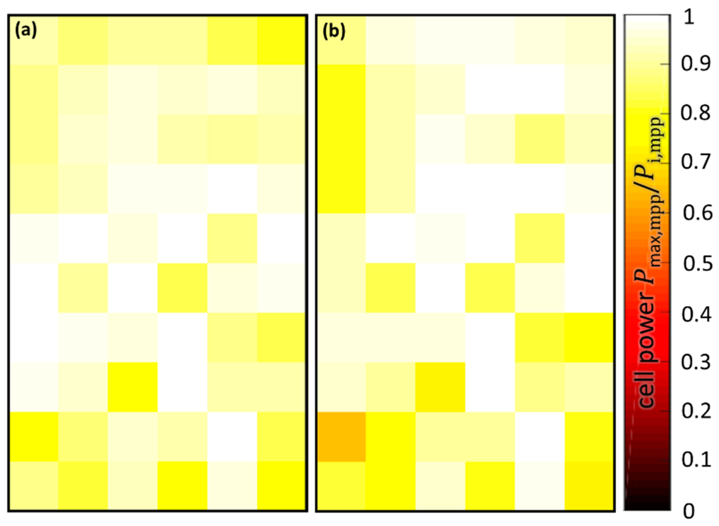
Based on the individual I/V curves, the maximal power of each cell i was extracted. Figure 7a shows the maximal power of the individual cells extracted from the I/V measurements, normalized to the maximal measured cell power in the module. Comparing the measured normalized cell powers of each cell i with the EL image in Figure 4a, the location of strongly damaged cells, indicated by dark regions in the EL images, matched the location of cells with low power output (dark yellow) in Figure 7a. The cells located at the top of the module in Figure 7a showed the strongest deviation, since there were no damaged cells in the EL images. However, this can be explained by the increased series resistance induced by the measurements (only in this case) using the junction box.
Comparing the measured results in Figure 7a with the simulated results in Figure 7b, initially using the ideality factor (lowest ideality factor from the expectation interval ), an excellent agreement between the normalized cell powers was found. Further, the maximal measured power of the total module = 209 W ± 5% (at STC) was also in good agreement with the simulated power expectation interval 200 W << 209 W, depending on the chosen ideality factor . The highest deviation was found for the ideality factor = 1, resulting in a maximal deviation of 4.3% compared to the measured power output. Since our I/V measurements usually showed an accuracy of ±5% for maximum power (at STC), these simulated results were already in the expected range of accuracy.
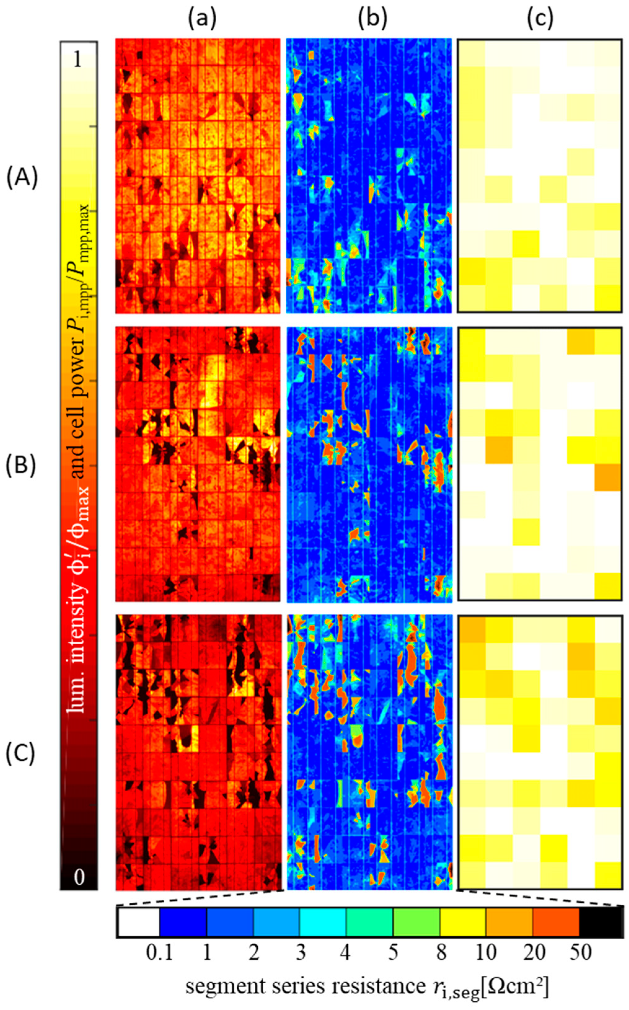
In addition to module A with open contacts at the backside of the modules, we further evaluated our method using two untreated modules of the same type (module B and module C). All three modules (A, B and C) were installed on the same site prior to the experiments and showed damage from hail-impact, with varying degrees of power loss. Figure 8 shows the resulting simulated power losses for all three modules using module A as the calibration module for the simulation.
As an additional calibration possibility aimed at a more accurate ideality factor approximation, we assumed that there was always access to one calibration module with a well-known I/V curve and not only data sheet information. Therefore, we used the already characterized I/V curve of module A to find the optimal ideality factor . The assumed ideality factor for calculating the series resistance map of module A was adjusted until the predicted power loss in the simulation showed a deviation to the measured I/V curve of MPP below 1%. The optimal ideality factor = 1.4 was then applied to predict the power loss of module B and module C.
Based on this calibration procedure, we found a deviation between the measured and simulated results for MPP power output below 1%. Table 1 summarizes the calibrated simulation results of all three characterized modules (A, B and C) with hail-damage from the same site.
3.2. PID Affected Module
As proof-of-concept of the parallel resistance approximation, we additionally evaluated EL images of a high-efficiency module (data sheet maximum power = 225 Wp) with 72 back-contact monocrystalline solar cells (cell area = 153 cm2) partially showing PID.
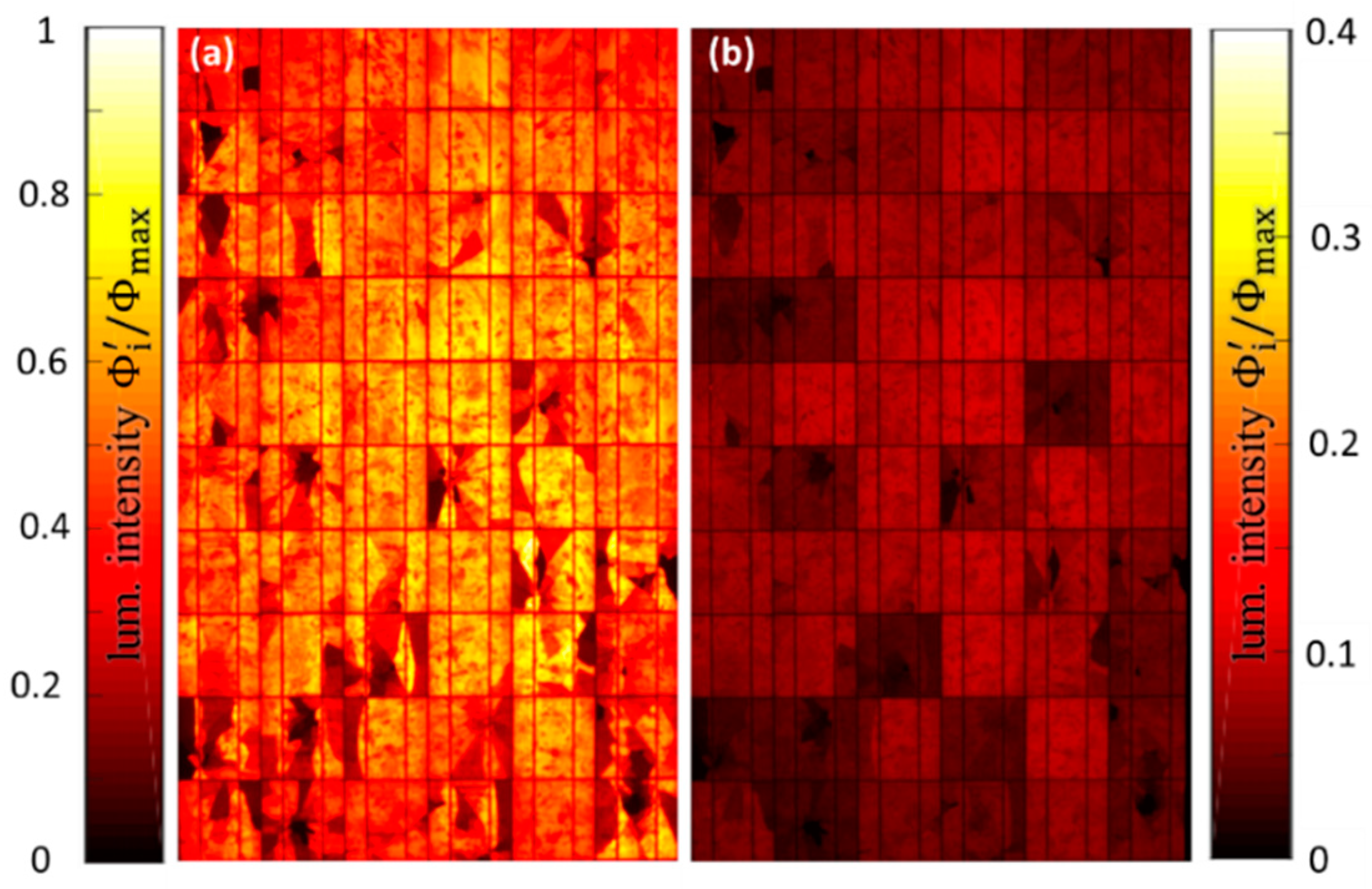
Figure 9a shows the low current (7% ) EL image of the PID module and the parallel resistance map of each cell i in Figure 9b. For PID only affecting the parallel resistance of cells, Equations (9) and (10) were used to directly calculate the parallel resistance from the mean luminescence of each cell i with the cell area . The result is shown in Figure 9b and was used to simulate the expected power output. Again, all other simulation parameters (, and ) were kept constant, assumed to be unaffected by the defect and were extracted from the data sheet.
By comparing the simulated results with the measured I/V curve, we found excellent agreement regarding the MPP power output with an error below 1% (measured power = 216 W and simulated power 217 W < < 218 W) using an ideality factor expectation interval .
4. Discussion
Regarding mechanically damaged modules with cracked solar cells, our modelling principle showed a clear physical relation between defect type and electrical characteristics based on common one-diode-modelling and already leads to very accurate power loss prediction. However, the limits of applicability with respect to the cells’ series resistances, as well as combination with shunts, need to be further evaluated.
In practice, the power loss of PID affected modules is evident, but the origin and specific types of PID are still under discussion. In the literature, there are several approaches for describing the origin of PID [2,9,10,11,12]. Typically, the resulting power loss is either linked to processes increasing carrier recombination due to degradation of the front side passivation layer, which increases the saturation current , or PID is modelled by simply decreasing the parallel resistance for shunt-type PID.
However, by solving Equation (8) analogously for the individual recombination currents using the mean luminescence of the individual cells, we found no clear correlation between measurements and simulations. Hence, we neglected the modelling approach based on a change in recombination current, and we described PID as a change in parallel resistance only, by using Equations (9) and (10).
5. Conclusions
This work presented a proof-of-concept of the novel electroluminescence characterization method ELMO based on series resistance mapping and modelling of photovoltaic modules with cracked solar cells. The series resistance map was successfully extracted from two luminescence images with low (<10% ) and high (>30% ) current injection. Using the data sheet information of the photovoltaic module, the simulation model was capable of predicting the expected power output with an error of less than 4.3%. By calibrating the ideality factor of the simulation using the I/V curve of the reference module, the error in the power loss prediction for the other modules of the same type was reduced to below 1%. By modelling PID as a change in parallel resistance, we approximated the power loss with an error of below 1% without any further calibration. The simultaneous application of parallel resistance approximation and series resistance mapping to predict power loss has yet to be evaluated. Furthermore, the impact of image quality on the simulation results needs to be analyzed.
Author Contributions
Timo Kropp developed the theory and simulation model, conducted the experiments and evaluated the data. Markus Schubert supervised the project and contributed with fruitful discussions and valuable suggestions. Jürgen H. Werner critically revised the theory and the paper. All authors contributed in writing the manuscript.
Acknowledgments
The authors would like to thank L. Stoicescu for helpful discussions. We gratefully acknowledge funding by the German Federal Ministry for Economic Affairs and Energy (BMWi) under contract No. 0324069A.
Conflicts of Interest
The authors declare no conflict of interest.
References
- Kajari-Schröder, S.; Kunze, I.; Eitner, U.; Köntges, M. Spatial and orientational distribution of cracks in crystalline photovoltaic modules generated by mechanical load tests. Sol. Energy Mater. Sol. Cells 2011, 95, 3054–3059. [Google Scholar] [CrossRef]
- Hara, K.; Jonai, S.; Masuda, A. Potential-induced degradation in photovoltaic modules based on n-type single crystalline Si solar cells. Sol. Energy Mater. Sol. Cells 2015, 140, 361–365. [Google Scholar] [CrossRef]
- Potthoff, T.; Bothe, K.; Eitner, U.; Hinken, D.; Köntges, M. Detection of the voltage distribution in photovoltaic modules by electroluminescence imaging. Prog. Photovolt. Res. Appl. 2010, 18, 100–106. [Google Scholar] [CrossRef]
- Fruehauf, F.; Turek, M. Quantification of Electroluminescence Measurements on Modules. Energy Procedia 2015, 77, 63–68. [Google Scholar] [CrossRef]
- Bauer, J.; Frühauf, F.; Breitenstein, O. Quantitative local current-voltage analysis and calculation of performance parameters of single solar cells in modules. Sol. Energy Mater. Sol. Cells 2017, 159, 8–19. [Google Scholar] [CrossRef]
- Köntges, M.; Kunze, I.; Kajari-Schröder, S.; Breitenmoser, X.; Bjorneklett, B. The risk of power loss in crystalline silicon based photovoltaic modules due to micro-cracks. Sol. Energy Mater. Sol. Cells 2011, 99, 1131–1137. [Google Scholar] [CrossRef]
- Quaschning, V.; Hanitsch, R. Numerical simulation of current-voltage characteristics of photovoltaic systems with shaded solar cells. Sol. Energy 1996, 56, 513–520. [Google Scholar] [CrossRef]
- Bishop, J.W. Computer simulation of the effects of electrical mismatches in photovoltaic cell interconnection circuits. Sol. Cells 1998, 25, 73–89. [Google Scholar] [CrossRef]
- Oh, J.; Bowden, S.; TamizhMani, G. Potential-Induced Degradation (PID): Incomplete Recovery of Shunt Resistance and Quantum Efficiency Losses. IEEE J. Photovolt. 2015, 5, 1540–1548. [Google Scholar] [CrossRef]
- Lausch, D.; Naumann, V.; Breitenstein, O.; Bauer, J.; Graff, A.; Bagdahn, J.; Hagendorf, C. Potential-Induced Degradation (PID): Introduction of a Novel Test Approach and Explanation of Increased Depletion Region Recombination. IEEE J. Photovolt. 2014, 4, 834–840. [Google Scholar] [CrossRef]
- Naumann, V.; Geppert, T.; Großer, S.; Wichmann, D.; Krokoszinski, H.; Werner, M.; Hagendorf, C. Potential-induced degradation at interdigitated back contact solar cells. Energy Procedia 2014, 55, 498–503. [Google Scholar] [CrossRef]
- Naumann, V.; Lausch, D.; Hähnel, A.; Bauer, J.; Breitenstein, O.; Graff, A.; Werner, M.; Swatek, S.; Großer, S.; Bagdahn, J.; Hagendorf, C. Explanation of potential-induced degradation of the shunting type by Na decoration of stacking faults in Si solar cells. Sol. Energy Mater. Sol. Cells 2015, 120, 383–389. [Google Scholar] [CrossRef]
Figure 1.
Equivalent circuit of each solar cell i in a PV module (a) and simplified circuit for an idealized solar cell () in the dark (0) (b). Mechanically damaged and cracked solar cells influence the junction voltage by means of a changed series resistance . In contrast, PID can be modeled as a change in parallel resistance of cell i and influences the junction voltage by reducing the current through the junction. The luminescence intensity results from the junction voltage .

Figure 2.
Equivalent circuit for referencing the local luminescence to the reference luminescence (), the highest luminescence intensity of cell i. The resistance cumulates the contact resistance as well as bus bar resistance between the individual cells. The local junction voltage generates the local luminescence () as part of to the cell voltage taking the voltage drop at each local series resistance into account. The reference luminescence () is generated by the local reference junction voltage .

Figure 3.
Equivalent circuit for referencing the mean luminescence of individual cells i (PID affected cells) to the cell with the maximal mean luminescence (best cell). The cell current density is identical for all cells connected in series and for each cell i divided into the current through the parallel resistance and the current density through the local diode.

Figure 4.
False color EL image of a hail-damaged photovoltaic module with 60 multicrystalline silicon solar cells (module A) at (a) supplied current of 37% of short circuit current 8.3 A with 100 s exposure time and (b) with 7% with 360 s exposure time. The local intensities in the low current EL image in (b) are downscaled proportional to the exposure time ratio. For the false color visualization, both images are normalized to the individual maximal luminescence intensity of the high current image in (a).

Figure 5.
False color segmentation of series resistance mapping (a). Predefined and separated into ten segments with the relative area as a share of the total cell area , all cells are individually modeled, as shown by the area segmentation histogram in (b). The model shown in (c) contains the series resistance segments and the constant diode model parameters extracted from the data sheet (green box). The ideality factor is identical for all cells and varied between . The reverse characteristics for describing the reverse current density depending on the breakdown voltage = −15 V as well as the breakdown model parameters 2.3 × 10⁻³ and = 1.9 are numerically modeled, as proposed by Quaschning [7]. From the data sheet, all other parameters are calculated, transposed into the series resistance map and scaled by the relative area of the segment. All cells i are connected in series and simulated with the bypass-diode configuration of the module.

Figure 6.
Measured irradiance (a) and temperature (b) during I/V curve acquisition of each cell i of a multicrystalline module with 60 cells (module A). (c) Calculated series resistance for each cell i from a two-diode equivalent circuit reproducing the measured I/V curve. All three values (, and ) illustrated in the images (a) to (c) were used to calculate the I/V curve at STC.

Figure 7.
Measured maximal power output (a) and simulated maximal power output (b) for all individual cells. All cell powers were normalized according to the maximal measured or simulated cell power in the module and colored by the same false color scale. The location of defective cells and the normalized cell power was in good agreement comparing simulation and measurement.

Figure 8.
Normalized false color EL images (a), calculated series resistance maps colored by categorized mean series resistance of segments (b) and simulated normalized power output of all cells of modules A, B and C (c). The simulated and normalized power output of cells identify the most severe defects in each module.

Figure 9.
False color EL image of a PID affected monocrystalline silicon photovoltaic module with back-contact solar cells at (a) supplied current of 7% with 300 s exposure time and (b) calculated parallel resistance map based on Equations (9) and (10).
Figure 9.
False color EL image of a PID affected monocrystalline silicon photovoltaic module with back-contact solar cells at (a) supplied current of 7% with 300 s exposure time and (b) calculated parallel resistance map based on Equations (9) and (10).


Table 1.
Calibrated simulation results of three multicrystalline modules (A, B and C) from the same site with hail damage. The calibration module A was used to determine the ideality factor = 1.4 as the optimal simulation setup ( ≈ ). The calibration of the ideality factor reduced error below 1% between the measured power and simulated power of modules B and C.
| Module Number | Measured Power [W] | Measured Power Loss p [%] | Calibrated and Simulated Power [W] |
|---|---|---|---|
| A | 209 W | 9.1% | 209 W |
| B | 198 W | 13.9% | 197 W |
| C | 186 W | 19.1% | 186 W |
© 2018 by the authors. Licensee MDPI, Basel, Switzerland. This article is an open access article distributed under the terms and conditions of the Creative Commons Attribution (CC BY) license (http://creativecommons.org/licenses/by/4.0/).
Share and Cite
MDPI and ACS Style
Kropp, T.; Schubert, M.; Werner, J.H. Quantitative Prediction of Power Loss for Damaged Photovoltaic Modules Using Electroluminescence. Energies 2018, 11, 1172. https://doi.org/10.3390/en11051172
AMA Style
Kropp T, Schubert M, Werner JH. Quantitative Prediction of Power Loss for Damaged Photovoltaic Modules Using Electroluminescence. Energies. 2018; 11(5):1172. https://doi.org/10.3390/en11051172
Chicago/Turabian StyleKropp, Timo, Markus Schubert, and Jürgen H. Werner. 2018. "Quantitative Prediction of Power Loss for Damaged Photovoltaic Modules Using Electroluminescence" Energies 11, no. 5: 1172. https://doi.org/10.3390/en11051172
Note that from the first issue of 2016, this journal uses article numbers instead of page numbers. See further details here.